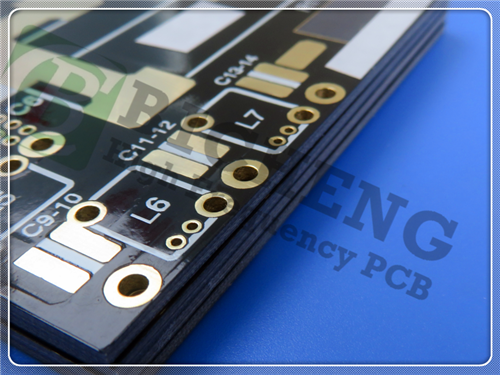
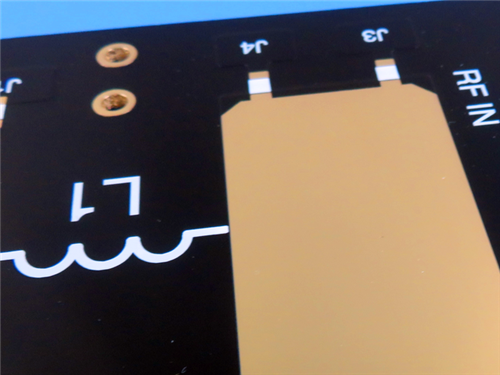
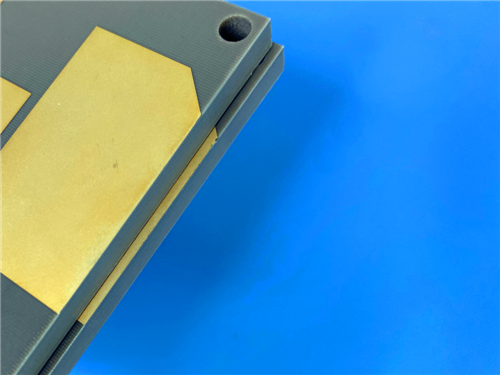
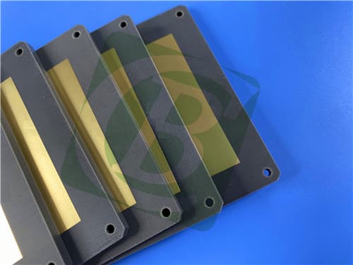
F4BTMS233 PCB 2-Layer 40mil Low Loss Material for Microwave and Phased Array Antennas1.F4BTMS Introduction The F4BTMS series represents an advanced version of the F4BTM series, showcasing significant technological advancements in material formulation and manufacturing processes. This series features a material enriched with a considerable amount of ceramics and reinforced with ultra-thin, ultra-fine glass fiber cloth, leading to notable enhancements in material performance and a wider range of dielectric constants. It is a high-reliability material designed for aerospace applications and can serve as a substitute for similar foreign products. By integrating a small quantity of ultra-thin, ultra-fine glass fiber cloth with a large amount of uniformly distributed special nano-ceramics mixed with polytetrafluoroethylene resin, the adverse effects of glass fiber on electromagnetic wave propagation are reduced. This innovation minimizes dielectric loss, enhances dimensional stability, and lowers the X/Y/Z anisotropy of the material. Additionally, it expands the usable frequency range, improves electrical strength, and boosts thermal conductivity. The material also features a low thermal expansion coefficient and stable dielectric temperature characteristics. The F4BTMS series includes RTF low roughness copper foil as a standard feature, which decreases conductor loss and provides excellent peel strength. It is compatible with both copper and aluminum bases. 2. Features (F4BTMS233) Dielectric constant (Dk) of 2.33 at 10GHz
3.PCB Stackup: 2-Layer Rigid PCB Copper Layer 1: 35 µm 4. PCB Construction Details Board Dimensions: 40mm x 108mm (1 piece, +/- 0.15mm) 5.PCB Statistics Components: 27 6.Type of Artwork Supplied Gerber RS-274-X 7. Quality Standard IPC-Class-2 8.Availability Worldwide 9. Typical Applications Aerospace equipment, space and cabin equipment |
Get a Quick Quote
Fill in the form below and our engineers will reply within 24 hours with technical specifications and pricing for F4BTMS233 PCB 2-Layer 40mil Low Loss Material for Microwave and Phased Array Antennas.
.jpg)
.jpg)
